Memory Market
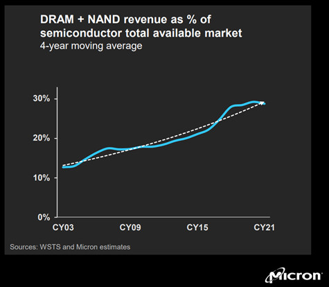
When reading industry publications this past year, the Micron Investor Day presentation really struck a chord. It did a particularly good job of outlining the current state of the DRAM industry, identifying changes on the horizon, and the corresponding drivers. One central theme throughout the presentation: an increasing need for DRAM technologies driven by a proliferation in data consumption that’s increasingly central to our daily lives. From IOT enabled washing machines to autonomous driving, our daily lives increasingly require the creation, communication, and management of vast amounts of data. The following chart shows the increasing importance of data through the expansion of DRAM +NAND share of the Total Available Market (TAM) within the overall semiconductor market.
Connectivity is King
The need for communicating large amounts of data with increasing speed requires innovation in DRAM technology, but that innovation must also come within the constraints of user experience needs. DRAM technology must not only be faster, but also be smaller and sleeker to fit within the necessary form factors that cater to end user needs. The following chart from Semiconductor Digest shows the ensuing increase in memory density that is necessary to cater to speed and style requirements.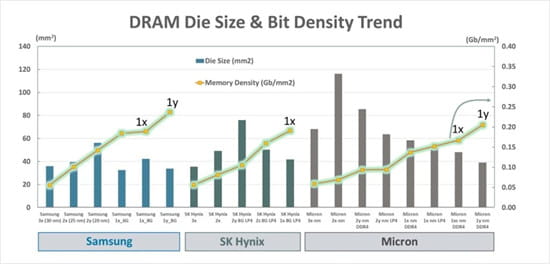
The issues in DRAM testing precipitated by this increased bit density fall into two key areas:
- Signal Access: Today’s smaller form factors require probe tips that can offer improved flexibility and reach to access difficult to reach test points
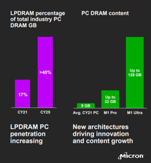
- Signal Integrity: Today’s high data rates require a probing setup that can transmit those fast signals with integrity, while maintaining a robust connection to the DUT for repeatability This jockeying for real-estate in the board layout has also brought with it an increase in demand for low-power DDR technologies. With the increasing technical capability of handheld devices, and the IOT-driven need to fit DRAM memory into increasingly unconventional devices, we see the LPDDR technologies becoming more prevalent. This comes with its own challenges; the low-power states those devices operate within require a probe tip with sufficiently lower circuit loading for the DUT to function normally.
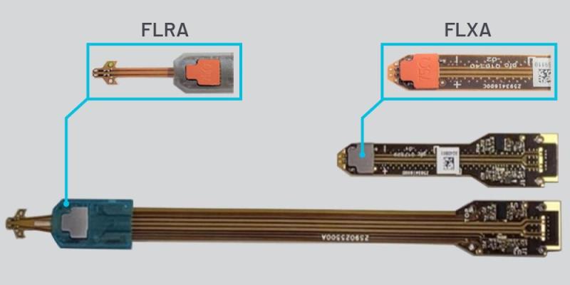
To address customer’s current and future DRAM testing needs, Tektronix recently released the P77STFLRA and P77HTFLRA probe tips.
Prized for their low noise and high signal fidelity, Tektronix’s P7700 probes and the P77STFLX* tip architecture have long been employed by our customers for memory testing as well as other general debug purposes. The active buffer amplifier on the tips provides superior low loading, which is critical to high-impedance measurements where accessing the signal without much interference is needed.(*The FLR tips employ similar naming convention to the FLX tips, where the A-version (FLXA or FLRA) is for general via & mid-bus probing, while the B-version (FLRB or FLXB) is for applications using an Interposer.)
Tektronix’s new FLR range of tips build upon the FLX architecture in many ways, but 3 key features enable them to deliver a superior probing experience for DRAM customers.Flexibility
Through the introduction of a new thinner, more flexible substrate layer, the FLR tips can provide unparalleled access in any given test setup. The improvement in minimum bend-radius over coax-based tips enables users to access difficult to reach test points found in increasingly smaller DUTs.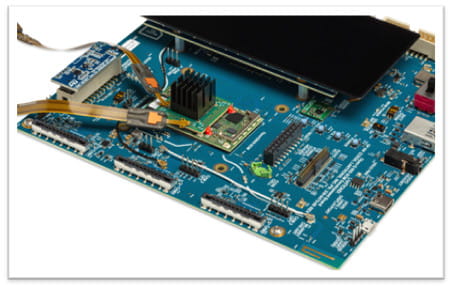
The FLR tips deliver a radical improvement in reach over the previous FLX tips and are built specifically to cater to the signal access issues presented by today’s DRAM testing. By significantly reducing the width of the point of the tip and increasing the length, we can fully leverage the flexibility of the new
Strain relief
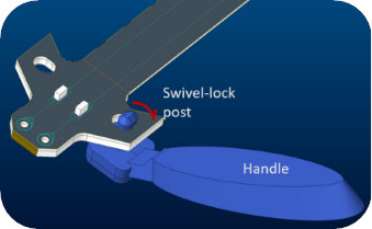
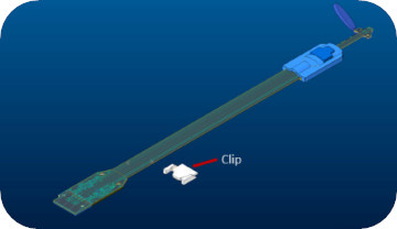
Our investigation on ways we could improve the DRAM testing workflow highlighted the fact that solder detachment is a key pain point in the workflow. We came to understand that providing better mechanical strain relief required not just a new probe, but also improvements to elements of the workflow. The increased flexibility of the tip could provide mechanical strain relief in the traditional sense, but the Kapton tape and hot glue that are ubiquitous to the DRAM testing workflow could be improved upon. To that end, Tektronix developed our LIGHTFOOT™ accessories.Our LIGHTFOOT accessories are a patented approach in providing additional mechanical strain relief. It includes a pair of plastic clips designed to help secure specific probe tips to the DUT; clips can be glued or taped down. We’ve worked with EMI on optimum adhesives. This offers a compact, repeatable way to preserve solder integrity vs the traditional Kapton tape approach.
Content Source: https://www.tek.com/en/blog/are-you-ready-for-whats-ahead-in-ddr-developing-new-tools-to-address-evolving-dram-testing-needs


